
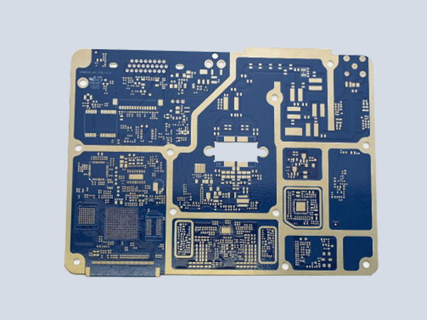
8 - layer communication PCB
Explore the 8 - layer communication PCB circuit board, a cutting - edge solution engineered for the demanding communication industry. With eight precisely crafted layers, this PCB offers superior performance and reliability. It is designed to meet the high - speed and high - density requirements of modern communication systems, making it an ideal choice for various communication applications. Whether it's for telecommunications networks, wireless devices, or data - communication equipment, this 8 - layer board can deliver exceptional results.
Product Description
- Layer Configuration
- The 8 - layer structure provides significantly more routing space and enhanced signal integrity compared to boards with fewer layers. This extra space allows for the implementation of more complex circuitry, which is essential for high - speed communication signals. The layers are carefully arranged to minimize signal interference and crosstalk, ensuring accurate data transmission. For example, power planes are strategically placed to supply stable power to components, while signal layers are designed to support high - frequency signals with minimal loss.
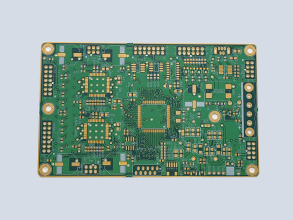
- High - Speed Signal Handling
- In communication applications, high - speed data transfer is crucial. The 8 - layer communication PCB is optimized to handle high - speed signals, such as those in 5G communication systems or high - speed Ethernet connections. Its design features controlled impedance traces, which help maintain signal quality over long distances. The board can support data rates of up to several gigabits per second, enabling seamless communication between different devices.
- Communication Applications
- This PCB is widely used in a variety of communication applications. In telecommunications networks, it can be found in base stations, where it processes and transmits large amounts of data. In wireless devices like smartphones and tablets, the 8 - layer PCB enables efficient communication with cellular networks and Wi - Fi hotspots. It is also used in data - communication equipment such as routers and switches, ensuring fast and reliable data transfer within local and wide - area networks.
- Reliability and Durability
- Built with high - quality materials, the 8 - layer communication PCB is highly reliable and durable. It can withstand the harsh environmental conditions often encountered in communication infrastructure, such as temperature variations, humidity, and electromagnetic interference. The board is designed to have excellent resistance to thermal cycling, ensuring that it can operate continuously without degradation in performance. Stringent quality control measures are implemented during manufacturing to guarantee that each board meets the highest standards.
- Customization Options
- Manufacturers offer customization services for the 8 - layer communication PCB. Whether you need specific component placements to fit the form - factor of your device, additional layers for more complex functions, or modifications to the signal routing to optimize performance for your unique application, customization can be tailored to your requirements. This flexibility allows you to create a PCB that is perfectly suited to your communication - related product.
Application Cases

Case Name
Case Name
Case Name
Case Name
Case Name


