
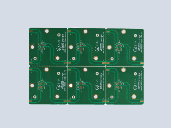
Multi - layer High - Frequency PCB
Discover the Multi - layer High - Frequency PCB, a cutting - edge solution in the world of printed circuit boards. Engineered with multiple layers and specialized for high - frequency applications, this PCB offers a host of advantages. It is designed to meet the demanding requirements of industries where high - speed data transfer and precise signal handling are crucial, such as telecommunications, aerospace, and automotive electronics. Whether you're developing 5G communication devices, satellite communication systems, or advanced automotive radar systems, this multi - layer high - frequency PCB can be the key to achieving optimal performance.
Product Description
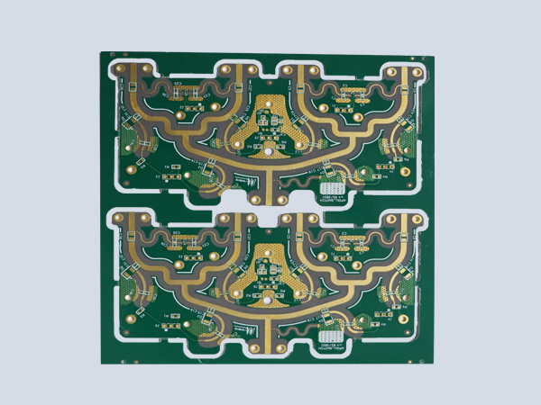
- Multi - layer Structure
- Enhanced Routing Capability: The multi - layer construction provides significantly more routing space compared to single - layer or double - layer PCBs. This extra space allows for the implementation of more complex circuitry, which is essential for high - frequency applications. Designers can separate power and signal layers more effectively, reducing interference and improving signal integrity. For example, dedicated power planes can be placed between signal layers to ensure stable power supply to components, while signal layers can be optimized for high - frequency signal transmission.
- Increased Component Integration: With multiple layers, more components can be integrated onto a single board. This not only leads to more compact designs but also reduces the need for external connectors and cables, which can introduce signal degradation. In aerospace applications, where space and weight are at a premium, the ability to integrate more components on a multi - layer PCB is highly advantageous.
- High - Frequency Performance
- Optimized for High - Frequency Signals: The multi - layer high - frequency PCB is designed to handle high - frequency signals with minimal loss and distortion. Its construction features controlled - impedance traces, which are crucial for maintaining signal integrity at high frequencies. The PCB can support frequencies ranging from several gigahertz to tens of gigahertz, making it suitable for applications such as 5G base stations, where high - speed data transfer and accurate signal processing are essential.
- Low Signal Delay: The carefully engineered layer stack - up of the multi - layer high - frequency PCB helps to minimize signal delay. This is crucial in applications where real - time data processing is required, such as in radar systems. By reducing signal delay, the PCB enables faster response times and more accurate detection of targets.
- Applications
- Telecommunications: In the telecommunications industry, multi - layer high - frequency PCBs are used in 5G base stations, fiber - optic communication equipment, and high - speed routers. These applications require high - density interconnects, high - speed data transfer, and reliable operation to meet the growing demand for faster and more reliable communication networks.
- Aerospace: In aerospace, multi - layer high - frequency PCBs are used in avionics systems, satellite communication equipment, and radar systems. The PCB's ability to handle high - frequency signals, withstand harsh environmental conditions, and provide reliable performance is essential for the safety and functionality of aircraft and spacecraft.
- Automotive Electronics: In the automotive industry, multi - layer high - frequency PCBs are used in advanced driver - assistance systems (ADAS), such as radar - based collision avoidance systems and in - vehicle communication systems. The PCB's high - frequency performance and compact design make it suitable for use in cars, where space is limited and high - speed data transfer is required for real - time processing of sensor data.
- Reliability and Quality
- High - Quality Materials: The multi - layer high - frequency PCB is constructed using high - quality materials that are selected for their excellent electrical, mechanical, and thermal properties. The laminates used in the board are designed to withstand high temperatures and provide good insulation, while the copper traces are of high purity to ensure low resistance and reliable electrical conductivity.
- Stringent Quality Control: The manufacturing process of the multi - layer high - frequency PCB involves strict quality control measures. Each layer is precisely fabricated and inspected to ensure accurate circuitry placement. The board undergoes comprehensive electrical testing, including impedance testing, continuity testing, and signal integrity analysis. Mechanical tests are also conducted to ensure that the PCB can withstand normal handling, installation, and the environmental conditions of its intended application. These rigorous quality control procedures guarantee that the PCB meets the highest industry standards.
- Customization Options
- Tailored to Your Needs: Manufacturers offer a wide range of customization options for the multi - layer high - frequency PCB. Whether you need specific component placements to fit a unique form - factor, additional layers for more complex functions, or customized routing designs to optimize performance for your application, the PCB can be tailored to your exact requirements. This flexibility allows you to create a PCB that is perfectly suited to your specific product, whether it's a new telecommunications device or an advanced aerospace system.
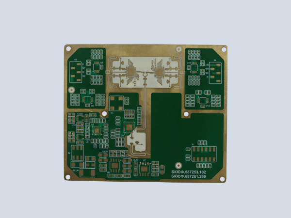
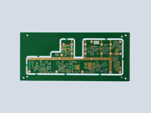
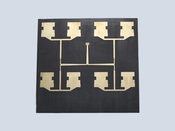
Application Cases

Case Name
Case Name
Case Name
Case Name
Case Name


