
6 - layer HDI Blind and Buried Via Circuit Board
Discover the 6 - layer HDI Blind and Buried Via Circuit Board, a high - performance and advanced solution in the realm of printed circuit boards. Engineered with six precisely designed layers and featuring high - density interconnect (HDI) technology along with blind and buried vias, this circuit board offers a multitude of benefits. It is tailor - made for applications that demand high - speed data transfer, compact design, and enhanced signal integrity. Whether you're in the fields of telecommunications, aerospace, or high - end computing, this 6 - layer HDI board can significantly boost the performance of your electronic systems.
Product Description
- Six - Layer Configuration
- Increased Routing Space: The six - layer structure provides a substantial amount of routing space, allowing for more complex circuitry designs. This is crucial for applications with high - density interconnect requirements. Designers can separate power and signal layers more effectively, reducing interference and optimizing signal integrity. For example, dedicated power planes can be placed between signal layers to ensure stable power supply to components, while signal layers can be customized for high - speed data transmission.
- Component Integration: With six layers, more components can be integrated onto a single board. This not only leads to a more compact design but also reduces the need for external connectors and cables, which can introduce signal degradation. In aerospace applications, where space and weight are at a premium, the ability to integrate more components on a 6 - layer PCB is highly advantageous.
- HDI Technology
- High - Density Interconnects: HDI technology enables the creation of smaller vias and traces, resulting in a higher density of interconnects on the board. This allows for the integration of more components in a limited space. In telecommunications devices, such as 5G base stations, the high - density interconnects provided by HDI technology are essential for handling the large number of connections required for high - speed data transfer.
- Improved Signal Integrity: The use of HDI technology helps to minimize signal interference and crosstalk. The closer proximity of components and the optimized routing of traces in HDI boards contribute to better signal integrity, especially at high frequencies. In high - end computing systems, where data transfer rates are extremely high, the improved signal integrity of HDI boards ensures accurate and reliable data transmission.
- Blind and Buried Vias
- Enhanced Circuit Design: Blind vias connect outer layers to inner layers, while buried vias connect inner layers to other inner layers. These types of vias eliminate the need for vias that penetrate through all layers of the board, reducing the overall board size and improving the routing efficiency. In applications where space is limited, such as in wearable electronics, the use of blind and buried vias allows for a more compact and lightweight circuit board design.
- Reduced Signal Loss: By reducing the length of the vias and minimizing the exposure of the signal paths to the external environment, blind and buried vias help to reduce signal loss. This is particularly important in high - speed data transfer applications, where even a small amount of signal loss can affect the performance of the system. In high - speed networking equipment, the use of blind and buried vias ensures that signals can be transmitted over long distances across the board with minimal degradation.
- Applications
- Telecommunications: In the telecommunications industry, 6 - layer HDI Blind and Buried Via Circuit Boards are used in 5G base stations, fiber - optic communication equipment, and high - speed routers. These boards are required to handle high - density interconnects, high - speed data transfer, and reliable operation to meet the growing demand for faster and more reliable communication networks.
- Aerospace: In aerospace applications, these circuit boards are used in avionics systems, satellite communication equipment, and flight control systems. The board's ability to handle complex circuitry, withstand harsh environmental conditions, and provide reliable performance is essential for the safety and functionality of aircraft and spacecraft.
- High - End Computing: High - end servers and supercomputers rely on 6 - layer HDI Blind and Buried Via Circuit Boards to support the high - speed data transfer and complex processing requirements of multiple processors, large amounts of memory, and high - bandwidth storage devices. The board's ability to integrate numerous components and provide excellent signal integrity is crucial for achieving maximum computing performance.
- Reliability and Quality
- High - Quality Materials: The 6 - layer HDI Blind and Buried Via Circuit Board is constructed using high - quality materials that are selected for their excellent electrical, mechanical, and thermal properties. The laminates used in the board are designed to withstand high temperatures and provide good insulation, while the copper traces are of high purity to ensure low resistance and reliable electrical conductivity.
- Stringent Quality Control: The manufacturing process of the board involves strict quality control measures. Each layer is precisely fabricated and inspected to ensure accurate circuitry placement. The board undergoes comprehensive electrical testing, including impedance testing, continuity testing, and signal integrity analysis. Mechanical tests are also conducted to ensure that the board can withstand normal handling, installation, and the environmental conditions of its intended application. These rigorous quality control procedures guarantee that the board meets the highest industry standards.
- Customization Options
- Tailored to Your Needs: Manufacturers offer a wide range of customization options for the 6 - layer HDI Blind and Buried Via Circuit Board. Whether you need specific component placements to fit a unique form - factor, additional layers for more complex functions, or customized routing designs to optimize performance for your application, the board can be tailored to your exact requirements. This flexibility allows you to create a circuit board that is perfectly suited to your specific product, whether it's a new telecommunications device or an advanced aerospace system.
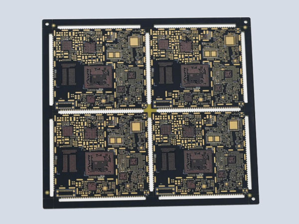
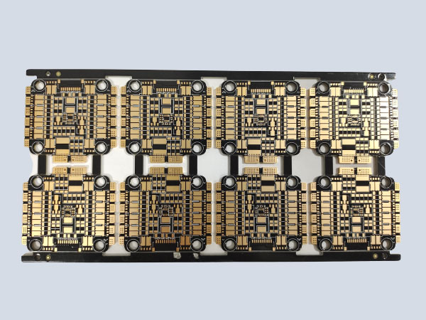
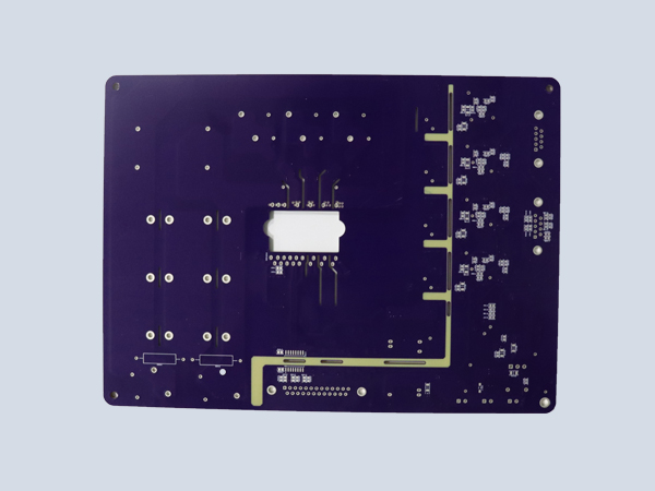
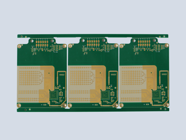
Application Cases

Case Name
Case Name
Case Name
Case Name
Case Name


