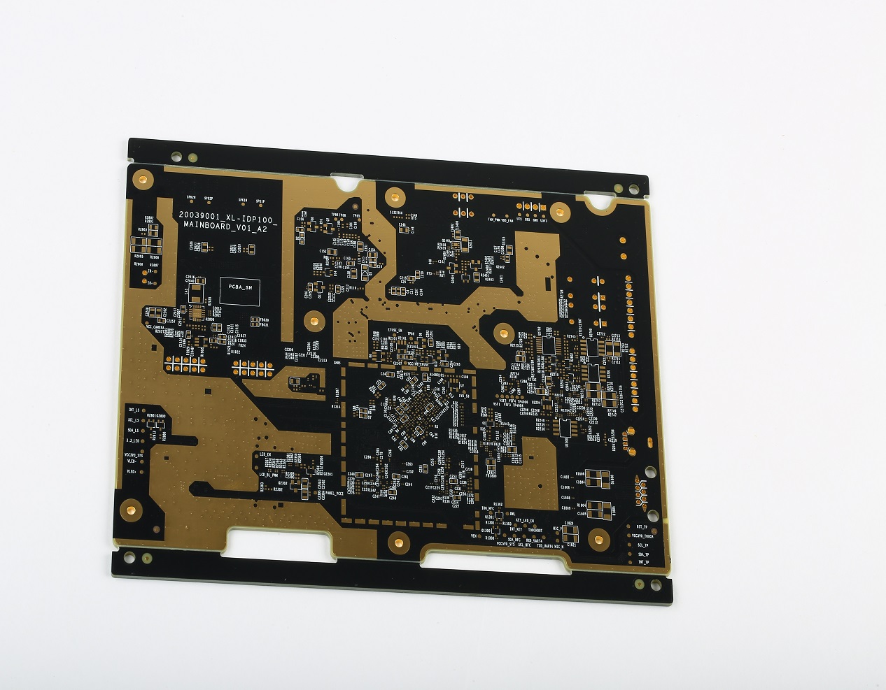
HDI Blind and Buried Via Circuit Board
Discover the HDI Blind and Buried Via Circuit Board, a high - performance solution at the forefront of printed circuit board technology. Leveraging High - Density Interconnect (HDI) techniques and incorporating blind and buried vias, this board offers a unique set of advantages. It's meticulously engineered to meet the stringent demands of industries that require compact designs, high - speed data transfer, and enhanced signal integrity. Whether you're in the telecommunications, aerospace, or electronics manufacturing sectors, the HDI Blind and Buried Via Circuit Board can be the game - changer for your projects, enabling the creation of advanced and reliable electronic devices.
Product Description
- HDI Technology
- High - Density Interconnects: HDI technology allows for the creation of smaller vias and traces. This results in a significantly higher density of interconnects on the circuit board. In applications such as smartphones, where multiple components need to be packed into a small space, HDI enables more efficient use of the available area. Smaller vias and traces also reduce the overall size of the board, contributing to more compact and lightweight device designs.
- Improved Signal Integrity: The closer proximity of components made possible by HDI helps in minimizing signal interference and crosstalk. With carefully designed trace routing and optimized impedance control, the board can handle high - frequency signals with minimal loss. In high - speed networking equipment, like 5G base stations, this is crucial for ensuring seamless data transfer at gigabit - per - second rates.
- Blind and Buried Vias
- Enhanced Circuit Design Flexibility: Blind vias connect outer layers to inner layers, while buried vias link inner layers to other inner layers. This eliminates the need for through - hole vias that penetrate all layers of the board. The use of blind and buried vias offers greater flexibility in circuit design. In medical devices, where space is at a premium and precise component placement is essential, these types of vias allow for more complex and efficient circuit layouts.
- Reduced Signal Loss: By shortening the length of signal paths and minimizing exposure to external interference, blind and buried vias help in reducing signal loss. In high - performance computing systems, where data needs to be transferred quickly between processors, memory modules, and storage devices, the reduced signal loss provided by these vias ensures accurate and fast data transmission, enhancing overall system performance.
- Applications
- Telecommunications: In the telecommunications industry, HDI Blind and Buried Via Circuit Boards are used in 5G base stations, fiber - optic communication equipment, and mobile devices. They support the high - density interconnects and high - speed data transfer requirements of modern communication technologies. In 5G smartphones, the board enables fast data download and upload speeds, smooth video streaming, and reliable connectivity for various applications.
- Aerospace: In aerospace applications, these boards are used in avionics systems, satellite communication equipment, and flight control systems. The ability of the board to withstand harsh environmental conditions, such as extreme temperatures, vibrations, and electromagnetic interference, makes it suitable for use in aircraft and spacecraft. The high - density interconnects and reliable performance are crucial for ensuring the safety and functionality of aerospace systems.
- Consumer Electronics: In consumer electronics like tablets, laptops, and smartwatches, HDI Blind and Buried Via Circuit Boards play a vital role. They allow for the integration of multiple components in a compact space, contributing to sleek and lightweight device designs. In a smartwatch, for example, the board can connect the display, processor, sensors, and battery in a small and efficient manner, enabling the device to offer a wide range of features in a wearable form - factor.
- Reliability and Quality
- High - Quality Materials: The HDI Blind and Buried Via Circuit Board is constructed using top - grade materials. The laminates are chosen for their excellent electrical insulation properties, mechanical strength, and thermal stability. High - purity copper is used for traces to ensure low resistance and reliable electrical conductivity. These materials are carefully selected to withstand the rigors of various applications and environmental conditions.
- Stringent Manufacturing Process: The manufacturing process of these boards involves strict quality control measures. Each layer is precisely fabricated and inspected to ensure accurate circuitry placement. The boards undergo comprehensive electrical testing, including impedance testing, continuity testing, and signal integrity analysis. Mechanical tests are also conducted to ensure that the board can withstand normal handling, installation, and the environmental conditions of its intended application. This ensures that the final product meets the highest industry standards.
- Customization Options
- Tailored to Your Needs: Manufacturers offer a wide range of customization options for HDI Blind and Buried Via Circuit Boards. Whether you need specific layer stack - ups to optimize electrical performance, customized shapes to fit unique device enclosures, or the integration of special components, the board can be designed and fabricated to your exact specifications. This flexibility allows you to create a circuit board that is perfectly tailored to your product, whether it's a new telecommunications device, an aerospace prototype, or a consumer electronics innovation.
Application Cases

Case Name
Case Name
Case Name
Case Name
Case Name


